Successful Cases &
Performance
Performance


|
Materials |
Substrate |
Materials Info |
Thickness |
Uniformity |
|
Proprietary SM OLED |
Glass |
4-6% Solids, 4-15cps |
20nm (.02 μm) |
3-4% |
|
Perovskite solution |
PV Glass |
PVK typical |
400-800nm |
2.0-5% |
|
PEDOT /HIL |
Glass |
2-5% |
60nm-200nm(0.06-0.2 μm) |
3% |
|
Proprietary Polyimide |
Stainless Steel-.003" |
35% Solids,300-1800cps |
0.97-7.0 μm |
3-4% |
|
DuPont 2611 Polyimide |
Glass |
13.5% Solids, 130 poise |
5 -25 μm |
3% |
|
Arch 115A Polyimide |
Wafer-300mm |
14.7% Solids,7574cs |
13.2 μm |
1.5% |
|
AZ SR110 Resist |
Glass |
11% Solids, 4cps |
1.5 μm |
2.8% |
|
AZ4620 Resist |
Glass |
42% Solids, 360 cps |
54 μm |
3% |
|
AZ4400 Resist |
Wafer -300mm |
37.2% Solids, 140csp |
10.3 μm |
1.8% |
|
PI/ PS PI |
FOPLP 515*510mm |
300CP |
35 μm |
2-4% |
|
Aqueous Dispersion |
Glass |
2 -5 μm particles |
5 - 10 μm |
3.4% |
|
Arch 7520 Durimide |
Wafer -150mm |
41% Solids, 6600cps |
20.7 μm |
2.6% |


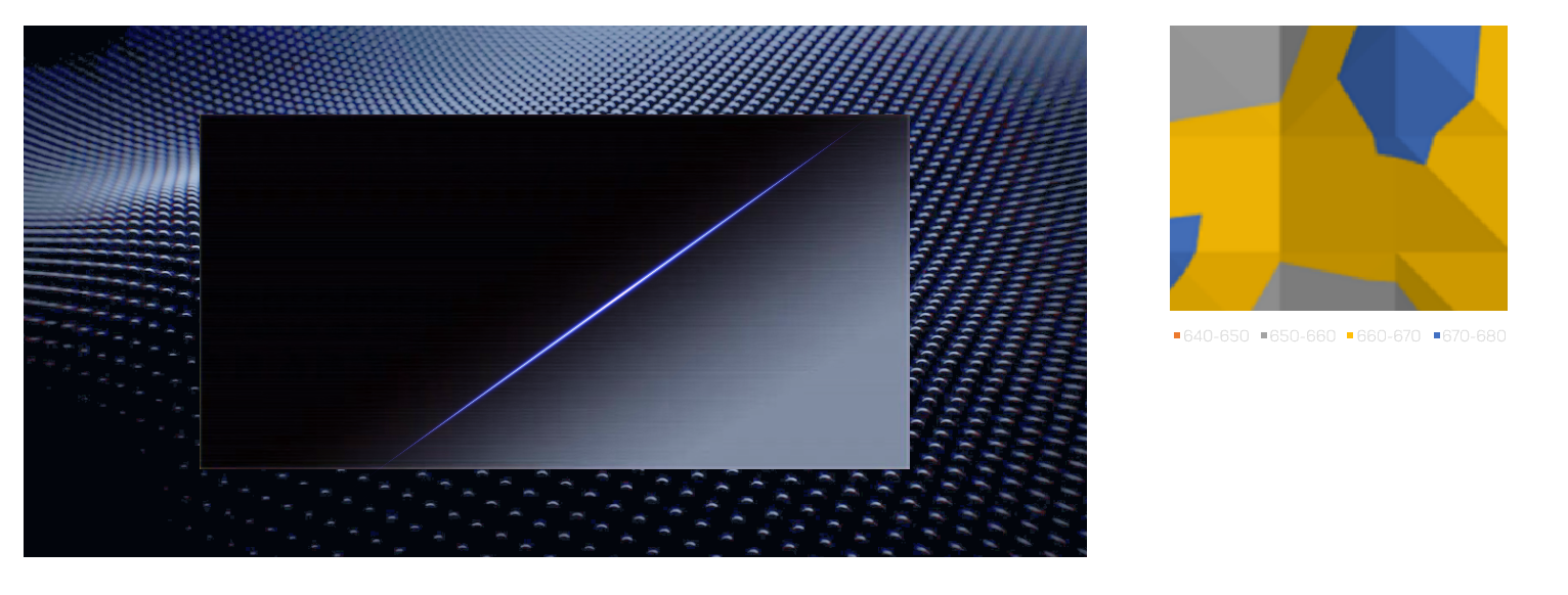
Single Junction panel 300mm*300mm
Coating thickens Uniformity : ±3% (E,E10mm) @ 550-600nm Target

.svg)
| Point | 1 | 2 | 3 | 4 | 5.. | 11 | 12 | 13 | 14.. | 20 | 21 | 22 | 23 | 24 | 25 | U±%<=±5% |
| 1th | 33729.86 | 33550.13 | 34003.63 | 33946.63 | 33969.39 | 35143.08 | 35284.46 | 34590.94 | 34971.96 | 35335.82 | 34977.29 | 35143.52 | 34739.69 | 35055.85 | 35092.58 | 2.58 |
| 2th | 33835.5 | 34045.97 | 33864.32 | 34106.05 | 34356.8 | 35493.11 | 35281.98 | 34960.62 | 35187.18 | 35503.06 | 34928.24 | 35060.56 | 34764.14 | 35004.57 | 35017.96 | 2.40 |
| 3th | 33564.86 | 33905.81 | 33527.97 | 33965.89 | 33545.82 | 35075.69 | 35156.78 | 34982.24 | 35253.58 | 35445.06 | 35175.23 | 35010.89 | 34571.7 | 34961.03 | 34977.98 | 2.77 |
| 4th | 34229.85 | 34824.36 | 33441.72 | 34451.48 | 34393.91 | 35169.15 | 35627.81 | 34910.8 | 36096.78 | 35358.42 | 35191.76 | 35689.94 | 35067.53 | 36092.22 | 35164.62 | 3.79 |
| 5th | 34092.29 | 34157.77 | 34357.56 | 34036.38 | 33531.82 | 34956.5 | 35242.62 | 34563.61 | 35160.99 | 35176.62 | 35076.41 | 35010.89 | 34647.02 | 35153.42 | 34934.96 | 2.47 |
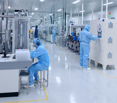
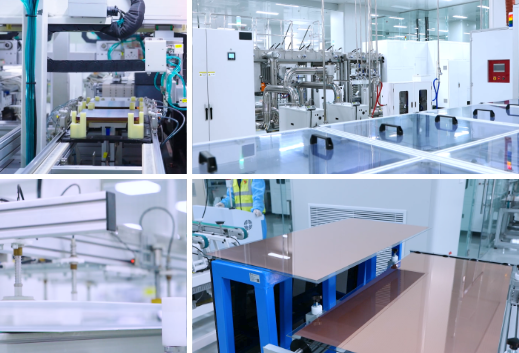
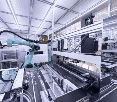
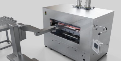
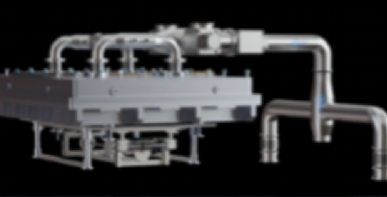
APS's new wet coating unit for advanced display has successfully been adopted by leading display companies for new display materials. On the customer's production line, the equipment's performance has been verified through long-term operation and fully meets customer standards. At the same time, APS has collaborated with multiple panel companies to test various advanced coating materials such as PSPI, photoresist, and PI, with performance fully matching the capabilities of international equipment. APS R&D department has also tested specialized materials for new display technologies, such as quantum dots and e-paper, with test results fully meeting the process requirements of new coating technologies.

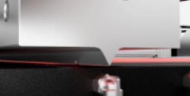
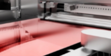
The CF process in TFT LCDs is primarily implemented using slot coating technology and equipment.
APS has several test centers for clients, please contact regional APS sales.